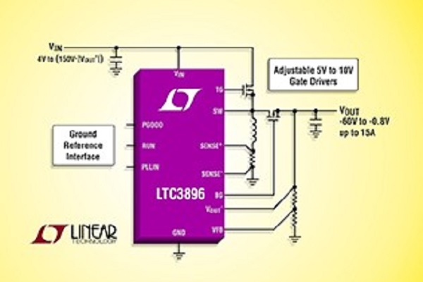
Linear Technology Corporation introduces the LTC3896, a high voltage inverting switching regulator controller that drives an all N-channel synchronous power MOSFET stage. Most low to medium power inverting DC/DC converters utilize a coupled inductor or transformer. However, the LTC3896 uses only a single inductor and converts a 4V to (150V – |VOUT‾|) positive input voltage to a regulated negative output voltage from -60V to -0.8V at output currents up to 15 amps. Efficiencies are as high as 96%, ideal for transportation, industrial, telecom and power distribution applications.
The LTC3896 contains true ground-referenced control pins, eliminating the need for discrete level-shifting components for its interface. This part draws only 40µA in sleep mode with the output voltage in regulation, ideal for always-on systems. The LTC3896’s powerful 1Ω N-channel MOSFET gate drivers can be adjusted from 5V to 10V to enable the use of logic- or standard-level MOSFETs to maximize efficiency. To prevent high on-chip power dissipation in high input voltage applications, the LTC3896 includes an NDRV pin, which drives the gate of an optional external N-channel MOSFET acting as a low dropout linear regulator to supply IC power. The EXTVCC pin permits the LTC3896 to be powered from its output voltage or other bias supply, which reduces power dissipation and improves efficiency.
The LTC3896 operates with an adjustable fixed frequency between 50kHz and 900kHz and is synchronizable to an external clock from 75kHz to 850kHz. The user can select from forced continuous operation, pulse-skipping or low ripple Burst Mode® operation during light loads. Its current mode architecture provides easy loop compensation, fast transient response and excellent line regulation. Current sensing is accomplished by measuring the voltage drop across the output inductor (DCR) for highest efficiency or by using an optional sense resistor. Current foldback limits MOSFET heat dissipation during overload conditions. Additional features include adjustable burst clamp and current limit, a power good output signal, an integrated bootstrap diode and adjustable soft-start.
The LTC3896 is available in a TSSOP-38 thermally enhanced package with several pins removed for high voltage spacing. Two operating junction temperature grades are available with extended and industrial versions from -40°C to 125°C and a high temp automotive version from -40°C to 150°C. The 1,000-piece price starts at $4.70 each. For more information, visit www.linear.com/product/LTC3896.
- VIN Range from 4V to (150V – |VOUT‾|)
- Wide VOUT Range: -60V to -0.8V
- Ground-Referenced Control/Interface Pins
- Adjustable Gate Drive Level 5V to 10V
- Requires Only One Inductor
- Integrated Bootstrap Diode
- Low Quiescent Current 40µA in Sleep Mode with Output in Regulation
- Onboard LDO or External NMOS LDO for DRVCC
- EXTVCC LDO Powers Drivers from Output
- Phase-Lockable Frequency (75kHz to 850kHz)
- Programmable Fixed Frequency (50kHz to 900kHz)
- Selectable Continuous, Pulse-Skipping or Low Ripple Burst Mode® Operation at Light Loads
- Power Good Output Voltage Monitor
- Programmable Input Overvoltage Lockout
38-Lead TSSOP High Voltage Package


