Record Performance Gate-All-Around InGaAs Nanowire FETs and InGaAs TFETs Presented at IEDM 2015
WASHINGTON – International Electron Devices Meeting 2015 (IEDM) – Dec., 2015—At this week’s IEEE IEDM conference, nano-electronics research center imec demonstrates record enhancement of novel InGaAs Gate-All-Around (GAA) channel devices integrated on 300mm Silicon and explores emerging tunnel devices based on optimization of the same III-V compound semiconductor.
III-V-on-Si GAA devices with a record peak transconductance at 0.5V has been achieved by optimizing both the channel epitaxy quality and the gate-channel passivation. In search of device technologies beyond FinFETs and GAA-nanowires for sub-0.5V operations, imec investigates InGaAs Tunnel-FET (TFETs). homo-junction III-V TFETs achieving a record ON-state current (ION) and superior subthreshold swing have been demonstrated. These results increase the knowledge on the impact of defectivity and channel optimization on device operations, and pave the way to advanced logic devices based on III-V-On-Si for high performance or ultra-low power applications.
Imec’s R&D program on advanced logic scaling is targeting the new and mounting challenges for performance, power, cost, and density scaling for future process technologies. One of the directions that imec is following, looks into beyond-Si solutions, such as integrating high-mobility materials into the channels of CMOS devices to increase their performance, and the integration challenges of these materials with silicon. Gate-All-Around Nanowire (GAA NW) FETs have been proven to offer significantly better short-channel electrostatics, and quantum-well FinFETs (with SiGe, Ge, or III-V channels) achieving high carrier mobility, are interesting concepts to increase device performance. Tunnel FETs, on the other hand, offering a steeper than 60mV/dec subthreshold swing, are a promising option for ultra-low power applications.
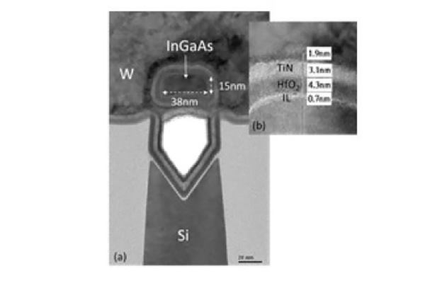
At IEDM, imec presented gate-all-around InGaAs Nanowire FETs (Lg=50nm) that performed at an average peak transconductance (gm) of 2200µS/µm with a SSSAT of 110mV/dec. Imec succeeded in increasing the performance by gate stack engineering using a novel gate stack ALD inter-layer (IL) material developed by ASM, and high pressure annealing. The novel IL/HfO2 stack achieved a 2.2 times higher gm for a device with a gate length (Lg) of 50nm, compared to the reference Al2O3/HfO2 stack.
Imec also presented a planar InGaAs homo-junction TFET with 70 percent Indium (In) content. The increase of In content from 53 to 70 percent in a 8nm channel, was found to significantly boost the performance of the device. A record ON-state current (ION) of 4µA/µm (IOFF = 100pA/µm, Vdd = 0.5V and Vd = 0.3V) with a minimum subthreshold swing (SSmin) of 60mV/dec at 300k was obtained for a planar homo-junction TFET device. It was also shown that subthreshold swing and transconductance in TFET devices were more immune to positive bias temperature instability (PBTI) compared to MOSFET devices.
“Imec’s R&D enables Moore’s law beyond the 5nm technology node through 3 approaches. First, we are tackling the technology challenges to extend silicon CMOS devices towards smaller nodes. At the same time, we research into disruptive heterogeneous solutions for beyond-silicon CMOS devices to increase performance and introduce new functionalities. Lastly, imec pursues emerging beyond-CMOS devices and systems such as spintronics to investigate further functional scaling beyond device-density-driven scaling,” stated Aaron Thean, vice president and director of imec’s advanced logic R&D program. “Boosting the performance of advanced compound semiconductor logic devices is extremely important, and these results support the quest of the semiconductor industry to find solutions that enable 5nm technology nodes and beyond.”
“ASM and imec have a long history of R&D collaboration using many of ASM’s products and advanced deposition and thermal processes,” says Ivo Raaijmakers, ASM CTO and Director of R&D. “As a leader in ALD, we are glad to see this breakthrough new ALD material now demonstrated in imec’s high mobility devices and presented at IEDM 2015.”
Imec’s research into advanced logic scaling is performed in cooperation with imec’s key partners in its core CMOS programs including GlobalFoundries, Intel, Micron, Panasonic, Qualcomm, Samsung, SK Hynix, Sony and TSMC.
TEM of complete gate-all-around InGaAs Nanowire FET and HRTEM of the gatestack


