At its annual Imec Technology Forum USA in San Francisco, imec, the world-leading research and innovation hub in nano-electronics and digital technology, today presented an electrically functional solution for the 5nm back-end-of-line (BEOL). The solution is a full dual-damascene module in combination with multi-patterning and multi-blocking. Scaling boosters and aggressive design rules pave the way to even smaller dimensions.
As R&D progresses towards the 5nm technology node, the tiny Cu wiring schemes in the chips’ BEOL are becoming more complex and compact. Shrinking the dimensions also reduces the wires cross-sectional area, driving up the resistance-capacitance product (RC) of the interconnect systems and thus increasing signal delay. To overcome the RC delay challenge and enable further improvements in interconnect performance, imec explores new materials, process modules and design solutions for future chip generations.
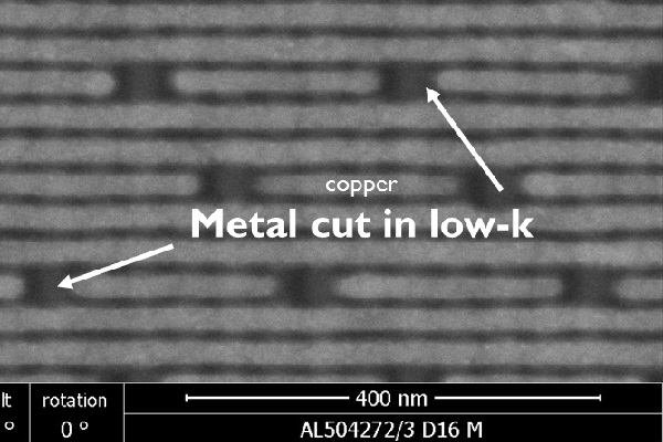
One viable option is to extend the Cu-based dual-damascene technology – the current workhorse process flow for interconnects – into the next technology nodes. Imec has demonstrated that the 5nm BEOL can be realized with a full dual-damascene module using multi-patterning solutions. With this flow, trenches are created with critical dimensions of 12nm at 16nm. Metal-cuts (or blocks) perpendicular to the trenches are added in order to create electrically functional lines and then the trenches are filled with metal. Area scaling is further pushed through the introduction of fully self-aligned vias. Moreover, aggressive design rules are explored to better control the variability of the metal tip-to-tips (T2Ts).
Beyond 5nm, imec is exploring alternative metals that can potentially replace Cu as a conductor. Among the candidates identified, low-resistive Ruthenium (Ru) demonstrated great promise. The imec team has realized Ru nanowires in scaled dimensions, with 58nm2 cross-sectional area, exhibiting a low resistivity, robust wafer-level reliability, and oxidation resistance – eliminating the need for a diffusion barrier.
“The emergence of RC delay issues started several technology nodes ago, and has become increasingly more challenging at each node. Through innovations in materials and process schemes, new BEOL architectures and system/technology co-optimization, we can overcome this challenge as far as the 5nm node”, said Zsolt Tokei, imec’s director of the nano-interconnect program. “Imec and its partners have shown attainable options for high density area scaled logic blocks for future nodes, which will drive the supplier community for future needs.”
For the longer term, imec is investigating different options including but not limited to alternative metals, insertion of self-assembled monolayers or alternative signaling techniques such as low-energy spin-wave propagation in magnetic waveguides, exploiting the electron’s spin to transport the signal. For example, the researchers have experimentally shown that spin waves can travel over several micrometers, the distance required by short and medium interconnects in equivalent spintronic circuits.
Imec’s research into advanced logic scaling is performed in cooperation with imec’s key partners in its core CMOS programs including GlobalFoundries, Huawei, Intel, Micron, Qualcomm, Samsung, SK Hynix, Sony Semiconductor Solutions and TSMC.


