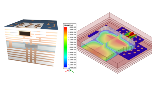
At this week’s International Microwave Symposium, imec – a world-leading research and innovation hub in nanoelectronics and digital technologies, and AT&S – a leading manufacturer of high-end printed circuit boards (PCBs) and IC substrates, present a major step towards realizing a novel system integration approach, whereby D-Band chips and waveguides are integrated into low-cost, mass-manufacturable PCBs. This new approach paves the way for the development of compact, cost-effective, and high-performance 140 GHz (automotive) radar and 6G mobile communications systems, offering significantly lower signal loss in comparison to planar PCB lines or substrate-integrated waveguides (SIWs) in PCBs and interposers.
The need for higher bandwidths in applications such as automotive radar and upcoming 6G mobile networks is fueling the demand for higher radio frequencies. This is why the D-Band, spanning from 110 to 170 GHz, garners significant attention.
But tapping into these frequencies poses challenges, such as increased system complexity and signal attenuation. Hollow air-filled substrate-integrated waveguide (AFSIW) technology with fully metalized sidewalls offers significantly reduced signal loss compared to substrate-integrated waveguides (SIWs) that use rows of vias and the planar interconnect technology used in current communication and radar systems. Despite this intrinsic benefit, a mass-production approach for PCBs with integrated AFSIW waveguides is currently unavailable.
Credit: Imec


