Designers of high-density electronics systems can now match 0.15 mm co-planarity connectors with 0.10 mm thick solder stencils through careful aperture design.
As electronic systems increase in component density, designers will typically look to match fine 0.10 mm thick solder paste stencils on the pc board to equally fine connectors with a co-planarity not in excess of 0.10 mm. However, a connector co-planarity value of 0.15 mm is not uncommon and it gets increasingly difficult to achieve 0.10 mm as the number of connector pins increases and with formed-pin, right-angle connectors. This has restricted designers’ connector options and either forced the use of multiple connectors when a single connector would have been preferred, or the use of stepped stencils. Both options add cost and complexity to the system design and production.
However, a study by Samtec Inc. and Phoenix Contact has shown that by optimizing the solder stencil aperture, designers can use the more widely available and less expensive 0.15 mm co-planarity connectors with the finer 0.10 mm stencils, while still meeting IPC-J-STD-001 Class 2 criteria for a 100% yield.
This article will discuss the relationship between stencils and connector co-planarity and the trade-offs and restrictions designers face. It will then describe the study, its results and the impact of those results with respect to design optimization for cost, space, performance, and reliability.
The stencil and connector co-planarity relationship
It’s not too difficult to precisely place a fine brick of solder paste using precisely machined stencils. However, it gets increasingly difficult to match the connector to that finely stenciled solder as the number of connector pins increases and where connector pins need to be formed and shaped, such as for right-angle connections. The main issue is the co-planarity of the connector pins.
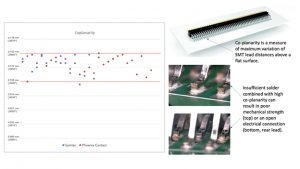
Roughly speaking, the term “co-planarity” refers to the maximum distance between the highest and the lowest lead, or pin, when the connector is sitting on a flat surface. It is typically measured using optical gauging equipment (Figure 1, left).
Figure 1: Co-planarity measures maximum lead height variation above a flat surface and it is critical to keep that variation to a minimum for SMT device leads to avoid problem joints (lower right). (Image source: Samtec Inc.)
Good co-planarity is critical for good solder joints: if a pin or lead is sitting too high, it may not make sufficient contact with the solder paste, resulting in a mechanically weak joint or a completely open electrical connection. Most specifications call for a co-planarity of between 0.10 mm and 0.15 mm.
With the right process and tools, it’s possible to consistently build connectors for most applications with co-planarity of 0.15 mm. However, a co-planarity of 0.10 mm is more difficult to achieve as pin counts increase and especially with advanced shaping and forming of the connector pins to specific angles, such as dual row, right angle. Maintaining this lower co-planarity can increase connector costs.
With large boards now comprising in excess of 3000 components and smaller, more integrated electronic devices forcing tighter space constraints (and as a result finer pitch components), designers are more frequently considering the use of 0.10 mm thick stencils. If the stencil is made any thicker, there is a higher risk of solder bridging between leads or pads. However, they are having difficulty finding connectors that meet the 0.10mmx co-planarity specification, with sufficient pin counts and suitable form factors.
Designers do have options, however. They can use a stepped stencil approach, with a thinner stencil for the fine pitch components and a larger stencil for the connector. This solves the problem, but at a higher stencil cost that may not fit applications where there isn’t sufficient space between components on either side of the step. The general rule of thumb requires a distance between stepped apertures of 36X the step thickness.
Another option is to use multiple connectors. Fewer pins make it easier for a connector to meet tighter co-planarity specifications. However, more connectors also add cost, as well as layout complexity and reliability issues. In addition, while a connector may meet 0.10 mm co-planarity requirements, a 0.10 mm stencil results in less solder volume, leading to a potentially weaker mechanical joint.
How to optimize the stencil aperture
To see if these tradeoffs can be minimized, Samtec and Phoenix Contact studied the effects of modifying the apertures of the stencil for three connector series. They used a 0.15 mm stencil with 1:1 aperture so the deposited solder was the same size and shape as the copper pad. They then added two variations of 0.10 mm stencils with enlarged apertures. Connectors were then built and selected for the study based on co-planarity values between 0.10 mm and 0.15 mm.
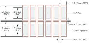
The study involved adjusting the aperture size beyond the size of the pad (overprinting) to increase the volume of solder and create a better connection, but not so much that it would cause bridging or leave solder balls on the board surface. To achieve this, the study relied upon the tendency of solder to coalesce on the heated pad once it has reached its liquidus temperature during reflow. Still, the right size aperture must be determined for each connector type (Figure 2).
Figure 2: The orange outline shows the optimal aperture dimensions for the FTSH connector. (Image source: Samtec Inc.)
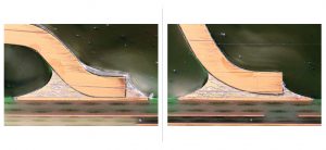
For instance, the optimal aperture to ensure a good solder joint between the sample FTSH connector, with a co-planarity of 0.152 mm, and the 0.10 mm stencil, is 2.84 mm X 0.97 mm. This results in a high-quality joint that meets IPC-J-STD-001 Class 2 criteria for a 100% yield (Figure 3).
Figure 3: A sample FTSH connector with a co-planarity of 0.152 mm soldered using a 0.10 mm thick stencil with optimized apertures shows a high-quality joint for both the inner (left) and outer (right) rows. (Image source: Samtec Inc.)
Based on these results, it’s clear that designers working with 0.10 mm stencils should give connectors with maximum co-planarity values of 0.15 mm a second look. If the optimum stencil aperture has been determined to allow the combination, this can open up a whole range of off-the-shelf connector options and avoid restrictive or expensive alternatives. If the optimum aperture is not available online or has not yet been determined, it’s important to contact the connector manufacturer early in the design process to either determine the optimum aperture or find a more suitable solution for any given application.
The key is to engage early. The further down the road a design has gone, the more limited the options.
Conclusion
Knowing the tradeoffs yet hearing customers’ call for ever finer stencils and tighter co-planarity, the research and development team at both Samtec Inc. and Phoenix Contact came together and found a way to optimize the stencil aperture such that connectors with 0.15 mm co-planarity can be used with 0.10 mm stencils. This result is the best of all worlds: fine 0.10 stencils, more connector options, low cost, low complexity, and mechanically strong joints that meet IPC-J-STD-001 Class 2 criteria.
David Decker
Director, Interconnect Processing Group
Samtec, Inc.
David Decker earned a Masters of Engineering degree in Mechanical Engineering from the University of Louisville’s Speed Scientific School in 1993 and acquired his Professional Engineering license in 1998. After beginning his career as an Injection Mold Tooling Engineer with Lexmark, Inc. and then General Electric Appliances, David moved on to Samtec where he has worked for 22 years holding positions in New Product design, Custom Product design and has been the Director of the Interconnect Processing Group for the last 15 years. David is also a Lieutenant in the Reserve Division of the Clark County Sheriff’s Office, where he has served for 9 years.


