At the 2017 European 3D Summit in Grenoble (France, Jan 23-25), the world-leading research and innovation hub for nano-electronics and digital technology imec and the leading supplier of wafer-bonding equipment EV Group (EVG) announce an extension to their successful collaboration, achieving excellent wafer-to-wafer overlay accuracy results in both hybrid bonding and dielectric bonding. Expanding this collaboration, EVG will become a partner in imec’s 3D integration program through a joint development agreement to further improve overlay accuracy in wafer-to-wafer bonding.
Wafer-to-wafer bonding is a promising technique for enabling high-density integration of future ICs through three-dimensional (3D) integration. This is achieved by aligning top and bottom wafers that are then bonded, thus creating a stacked IC. An important advantage is that wafers/ICs with different technologies can be stacked, e.g. memory and processor ICs.
Many of the alignment techniques and bonding methods for 3D integration have evolved from microelectromechanical system (MEMS) fabrication methods. The fundamental difference between MEMS and 3D integration is that the alignment or overlay accuracy has to be improved by 5–10 times. Accurate overlay is needed to align the bonding pads of the stacked wafers and it is essential to achieving a high yield with wafer-to-wafer bonding. Imec and EVG have realized excellent results on overlay accuracy.
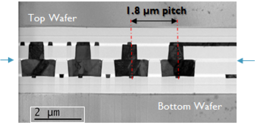
Firstly, the hybrid (via-middle) wafer-to-wafer bonding technique was improved by using EVG’s high quality bonding system with beyond state-of-the-art integration definition of bonding pads, resulting in a high yield and a 1.8µm pitch, which is significantly better compared to recently published results at recognized conferences such as ECTC and 3DIC reporting 3.6µm pad size.
Secondly, the dielectric (via-last) wafer-to-wafer bonding technique was tackled. This technique requires extremely good overlay accuracy to align the copper pads from both wafers, which are then contacted by through-silicon vias (TSVs). In this case, 300nm overlay across the wafer was achieved.
“By joining forces, we achieved these excellent results on overlay accuracy,” explains Eric Beyne, fellow at imec. “We are excited that we can expand our collaboration with EVG with a JDP and the installation of EVG’s GEMINI FB XT wafer bonder in our cleanroom. The GEMINI FB XT has the potential to further reduce the wafer-to-wafer overlay errors and therefore allow for the development of sub-micron wafer-to-wafer interconnects technologies.”
“Further improving the overlay accuracy for wafer-to-wafer bonding into the sub-200nm range requires optimization of the interaction between the wafer bonding tool and processes as well as pre-and post-processing and the wafer material,” explains Markus Wimplinger, corporate technology development & IP director at EVG. “We are excited to partner with imec in an effort to advance overlay accuracies for wafer-to-wafer bonding to meet the needs of future 3D IC designs that rely on high density interconnects”
Imec’s 3D integration program explores technology options to define innovative solutions for cost-effective realization of 3D interconnect with TSVs. Imec’s 3D integration processes are completely executed on 300mm. Imec also explores 3D design to propose methodologies for critical design issues, enabling effective use of 3D interconnection on system level.


