Introduction
David Morrison of How2Power magazine recently asked several smart power supply engineers about their interest in power integrity (PI) at APEC. The surprising responses revealed a recurring misconception about PI and who is ultimately responsible for it.
The majority of responses indicated that power supply engineers were not particularly interested in PI, since it’s a system level issue and not a power supply issue. Power Integrity is NOT a system level issue and this one misconception will get you. When it does, it will cost you and/or your company big bucks.
An Analogy
This misconception is analogous to believing that high speed and microwave engineers don’t need to worry about impedance matching as that’s a system level issue. In the case of RF, most circuits maintain a 50Ω impedance. The source is 50Ω, the load is 50Ω and the interconnecting printed circuit boards and cables are 50Ω. The impedance matching is well understood and designers of each circuit stage plan for this in their design. The PCB designer also assures that the traces maintain the 50Ω impedance necessary to match the source and load circuits. The same is true of high speed differential transceivers, though the impedance levels tend to be higher, often 100Ω. While power systems are not nearly so well defined, the same considerations are warranted.
What is PI?
Power integrity is the assurance that appropriate power is delivered to the circuits within this system. Appropriate is dependent on what is being powered. For example, low noise microwave amplifiers (LNA’s), low jitter clocks and analog sensors can be sensitive to microvolts of power supply noise. This is quite different from high speed transceivers and FPGA’s that must maintain certain operating voltage levels, despite very large operating current transients. Power integrity is the assurance that these various power quality requirements are met at each circuit throughout the system. It’s easy to see then why it might be incorrectly perceived as a system level issue. But the fact remains it is not a system level issue. The power supply plays a very large role in PI and overcoming an inappropriate power supply may be expensive at best and insurmountable at worst.
What is the PDN
The power system is comprised of power supplies, printed circuit board planes and decoupling capacitors. Collectively, these represent the power distribution (or delivery) network (PDN) as seen in Figure 1. These individual elements interact with each other and achieving PI requires them to be properly balanced.

Figure 1 The Power Distribution Network (PDN) is comprised of the VRM, planes and decoupling capacitors
That being the case the characteristics of the power supply have a significant impact on PI and counter-intuitively a power supply that is “too good” can destroy the balance, resulting in significantly degraded PI.
The power supply contribution to PI
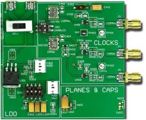
The Picotest VRTS3 training board includes just such an example. The section of the board shown in Figure 2 includes a linear regulator with a selection of output capacitors (U301 and C301-C304), a printed circuit board trace and a 10nF local decoupling capacitor, C402. resulting power is applied to a 125MHz clock (OSC401).

Figure 2 A section of the Picotest VRTS3 training board include an LDO (U301), bulk capacitors (C301-C304), a decoupling capacitor (C402) and a 125MHz clock (OSC401). The connections are made by PCB traces.
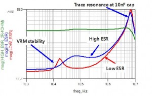
The power supply impedance is measured at the decoupling capacitor in order to see the power quality at the load (125MHz clock) and shown in Figure 3. The impedance is measure with 2 different LDO output capacitors and also with a 2.4Ω resistor switched in series between the voltage regulator and the decoupling capacitor. Yes, the insertion of the resistor significantly degrades the voltage regulation of the LDO and yet, the impedance seen at the clock is much lower with the series resistor added. This is the result of matching the impedance of the VRM (in this case it is our LDO) with the impedance of the circuit board and decoupling capacitor.
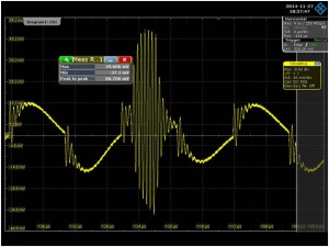
The impedance in the red trace is with a low ESR capacitor that results in an impedance peak at approximately 15MHz due to poor control loop stability. A second peak appears at approximately 7MHz and is the result of the net inductance of the PCB trace resonating with the local decoupling capacitor (C402). Since there are two peaks, it is possible to generate a rogue wave by exciting both resonances simultaneously as seen in Figure 4.

Figure 3 The impedance is measured at the clock decoupling capacitor (C402) with 2 different output capacitors and with a 2.4Ω resistor switched in series between the LDO and the decoupling capacitor.
Certainly there are alternative methods of correcting this deficiency. One possibility is to replace the 10nF capacitor with a larger decoupling capacitor. In this case, using the High ESR regulator output capacitor and replacing the 10nF decoupling capacitor with 0.47uF with a 0.5Ω ESR would also eliminate the peak. The capacitor likely needs to be closer to 1uF to overcome the DC bias effect of the ceramic capacitor. This solution adds more parts and the 0.47uF ceramic might be significantly larger. Another possibility is to move the regulator closer to the clock and possibly increase the width of the PCB trace or reduce the dielectric thickness of the PCB. The point is that the power supply, PCB and system have to be designed as a unit. Designing a power supply in isolation of the system will only pass the problems on to someone else where it will ultimately result in a more costly solution.
Selecting a lower cost and higher ESR capacitor results in the blue trace. The first sharp resonance has been eliminated and note that while the ESR increased the impedance at C402 is now lower than with the low ESR capacitor. The peak is still large since the VRM output resistance is much lower than the characteristic impedance of the PCB and decoupling capacitors.

Figure 4 creating a load step that excites the forced resonance at the lower frequency, followed by an appropriately timed burst at 7MHz results in a rogue wave with peak to peak voltage exceeding either resonance.
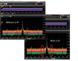
The clock spectrum is shown in Figure 5 with and without the 2.4Ω series resistor switched in. Without the series resistor, the clock shows strong 7MHz sidebands while these sidebands are eliminated by switching in the 2.4Ω series resistor.
Conclusion
Power integrity might be misconceived as a system issue, however, as we have shown the voltage regulator and the system interact with each other.
A well planned PDN saves time and money, as well as a great deal of aggravation and stress. The power supply, printed circuit board and circuits being powered are generally designed independently and on different time schedules. Nonetheless, it is important to determine the general power characteristics required by the load circuits. The primary

Figure 5 The clock spectrum shows strong sidebands at 7MHz without the series resistor switched n and these sidebands are eliminated when the series resistor is switched in.
characteristics include the voltage level and accuracy, ripple and noise voltage, operating load current and dynamic load current transients. These characteristics will help in determining the power supply impedance, printed circuit board plane impedance, decoupling networks.
References
More references here
Mastering Power Integrity Webinar https://www.keysight.com/main/eventDetail.jspx?cc=US&lc=eng&ckey=2622154&nid=-34466.0&pid=1420492


