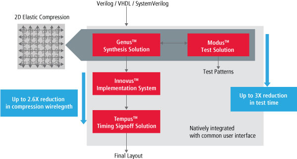

The new Modus Test Solution with its patent-pending, physically aware 2D Elastic Compression architecture integrated into the Cadence digital flow.
Physically aware 2D Elastic Compression architecture reduces test logic wirelength by up to 2.6X and enables compression ratios to scale beyond 400X without impacting design size
Cadence Design Systems, Inc. (NASDAQ: CDNS) today announced the new Modus™ Test Solution that enables design engineers to achieve an up to 3X reduction in test time, thereby reducing production test cost and increasing silicon profit margins. This next-generation test solution incorporates patent-pending, physically aware 2D Elastic Compression architecture that enables compression ratios beyond 400X without impacting design size or routing.
To address the challenges that come with testing designs, the Cadence® Modus Test Solution includes the following innovative capabilities:
“Our next-generation Modus Test Solution delivers new, innovative patent-pending technology that fundamentally changes the way design and test engineers address the test problem,” said Dr. Anirudh Devgan, senior vice president and general manager of the Digital and Signoff Group at Cadence. “By using a physically aware approach in a 2D grid, and compressing patterns sequentially as well, the Modus Test Solution can significantly reduce digital test time in comparison to traditional approaches, thereby giving Cadence customers yet another significant profitability advantage.”
For more information on the Modus Test Solution, please visit www.cadence.com/news/modus.
Customer Endorsements
“The Modus Test Solution demonstrated a 3.6X reduction in test time on a customer networking chip without impacting design routability or fault coverage. This technology definitely reduces production test costs. The evolution of the Modus Test Solution, as well as the Innovus Implementation System, the Tempus Timing Signoff Solution and the Voltus™ IC Power Integrity Solution, provides a leading-edge end-to-end design flow in 14nm and beyond for our worldwide design centers and for our ASIC customers. ”
-Sue Bentlage, director, ASIC design and methodology at GLOBALFOUNDRIES
“Minimizing the cost of test is crucial in high-volume, price-sensitive markets like embedded processing. The Modus Test Solution is showing a 1.7X reduction in digital test time on one of our largest and most complex embedded processor chips without any impact on design closure.”
-Roger Peters, MCU silicon development at Texas Instruments
“With the Modus Test Solution, we achieved an impressive 2.6X reduction in compression wirelength and a 2X reduction in scan time. The reduction in compression logic wirelength enabled us to address a key challenge for design closure as we push to smaller process nodes and scale design size.”
-Alan Nakamoto, vice president, engineering services at Microsemi Corp.
“Test time has a significant impact on semiconductor product costs and production capacity, so reducing test time is important. We have seen the Modus Test Solution achieve a 2X reduction in test time without impacting fault coverage or die size.”
-Chris Malkin, baseband IC manager at Sequans
Infineon further strengthens its number one position in automotive microcontrollers and boosts systems capabilities for…
Rohde & Schwarz has achieved a significant milestone, receiving approval of detection capability from the…
April 8, 2025 - Avnet ASIC, a leading provider of ASIC and SoC full turnkey…
Acquisition expands Siemens’ offering in PCB design for the SMB market and enables greater process…
Wireless Communication Modules in innovative LED lighting systems Panasonic Industry Europe is proud to announce…
Company expands AI order-taking solution to tackle rising labor costs and improve customer experience Hi…