New PSoC® 4 L-Series Reduces Costs and Gets Embedded Designs to Market Faster with the Ability to Develop Premium User Interfaces and Product Variations Rapidly
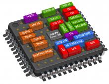
Cypress Semiconductor Corp. (Nasdaq: CY) today introduced a new series from its PSoC® 4 programmable system-on-chip architecture. The new PSoC 4 L-Series is the industry’s most integrated single-chip solution with a 32-bit ARM®-Cortex®-M0 core, adding up to 256KB flash memory, 98 general purpose I/Os, 33 programmable analog and digital blocks, a USB device controller, and a control area network (CAN) interface. The PSoC 4 L-Series is ideal for a broad range of industrial and consumer applications, leveraging the flexibility of the PSoC architecture to address multiple product variations and Cypress’s industry-leading CapSense® capacitive touch-sensing technology to implement reliable and elegant user interfaces.
“The award-winning PSoC 4 portfolio has enabled customers to easily migrate from proprietary 8-bit and 16-bit MCUs to the industry’s most integrated ARM Cortex-M0 System-on-Chip,” said John Weil, vice president of MCU marketing at Cypress. “The PSoC 4 L-Series introduces new capabilities such as dual-mutual CapSense blocks with up to 94 channels for large, capacitive-touch home appliance applications and USB and programmable digital blocks to create bit-perfect digital audio solutions. Additionally, it provides all the resources needed to create new products for the emerging USB Type-C market.”
The PSoC 4 L-Series delivers up to 13 programmable analog blocks including 4 high-performance opamps, 4 current-output digital-to-analog converters (IDACs), 2 low-power comparators, a 12-bit SAR ADC and dual CapSense blocks with up to 94 capacitive-sensing channels. The programmable analog blocks enable engineers to create on-chip, custom analog front ends to support new end-product features, without increasing product costs, size or power consumption.
The PSoC 4 L-Series delivers up to 20 programmable digital blocks including 8 timer/counter/PWM blocks, 4 serial communication blocks and 8 Universal Digital Blocks (UDBs)—programmable digital blocks that each contain two programmable logic devices, a programmable data path and status and control registers. UDBs can be configured as coprocessors to offload compute-intensive tasks from the ARM Cortex-M0 core. The blocks also enable engineers to implement custom digital peripherals, state machines or glue logic. Traditional MCUs typically require additional ICs to implement this functionality.
The scalable PSoC 4 architecture is complemented by the easy-to-use PSoC Creator™ Integrated Design Environment (IDE), which simplifies system design and accelerates time-to-market by enabling concurrent hardware and firmware design, and PSoC Components—free embedded ICs represented by an icon in the IDE. Together they enable rapid prototyping of end applications while minimizing PCB spins and firmware changes that are typically required.
Availability and Photo
The PSoC 4 L-Series is currently sampling with production expected in the first quarter of 2016. Parts will be available in 48-pin TQFP, 64-pin TQFP, 68-pin QFN and 124-pin VFBGA packages from Cypress and its authorized distributors. Learn more about the PSoC 4 portfolio at www.cypress.com/PSoC4. A graphic for PSoC 4 L-Series appears below.


