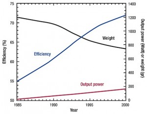
Advances in semiconductor technology and component integration have played a significant role in reducing SWaP.
Defense and commercial airborne platforms differ in many ways: Defense platforms focus on multifunction systems and power management for mission-critical functions such as electronic warfare, fire control, radar, etc., while commercial aircraft place high emphasis on safety and system redundancy. One area of common concern for both is maximizing payload efficiency. Every ounce of weight, cubic centimeter of space, and milliwatt hour of power is carefully planned, as both focus on balancing size, weight and power (SWaP). Advances in RF technology can provide a leapfrog advantage for manned and unmanned aircraft in both markets.
SWaP refers to arguably the most important specification in new product, project, or platform definition from electronic warfare to avionics. Nearly all new developments – whether shipboard, airborne, terrestrial, man-carried, or carried in hand – share a common requirement: Make it smaller, make it use fewer resources, and make it contribute more to the overall system functionality. A lean system is more desirable in the current social, economic, political, and global environments. Lately, SWaP increasingly seems to be the key driving factor, providing difficult tradeoffs over system performance enhancements and multifunction architectures.
Culprit identification
Let us take a look at a few of the miscreants, scandalous offenders, and substantially burdensome characters.
Copper is the conductor of choice for electrical power transmission. A thousand feet of AWG 5 gauge copper wire without insulation weighs nearly 100 pounds (50 kg). To add insult to injury, the inherent resistance of wire causes electrical current to be wasted in the form of dissipated heat. The next perpetrator in the lineup is legacy component size. Consider the case of the shipboard radar local oscillator (LO); the LO feeds both the transmitter and receiver. The LO must produce a stable frequency with low harmonics, while the highest-stability requirements must account for temperature, voltage, and mechanical drift. The oscillator must produce enough output power to effectively drive subsequent stages of circuitry, such as mixers or frequency multipliers. It must have low phase noise where the timing of the signal is critical. Historically, the LO was generated and distributed by separate and specially designed subsystems. The same or similar was true for airborne systems: Large size, power-hungry, and heavy due to the solid-state component content.
The legacy component that has provided high-power radio frequency (RF) to a system is the traveling wave tube (TWT), which is a specialized vacuum tube that is used in electronics to amplify RF signals in the microwaverange range (Figure 1). The bandwidth of a broadband TWT can be as high as one octave, although tuned (narrowband) versions are more common; operating frequencies range from 300 MHz to 50 GHz. These TWT systems are somewhat efficient, but they are a single point of failure; reliability is a significant concern with TWTs. Microwave tube reliability is strongly dependent on three factors. First, defects introduced during the manufacturing process adversely affect reliability, with concerns about production problems, poor workmanship, and lack of process control. Secondly, tube reliability is heavily dependent upon operating procedures and handling. Finally, adequate design margin must exist between the operating point and the ultimate design capability of the tube in order to have reliable operation. These are just three examples of the many enemies of SWaP.
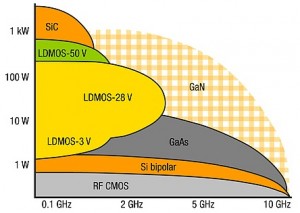
Advances in semiconductor technology and component integration have played a significant role in reducing SWaP. Solid-state power amplifiers (SSPAs) are not a new technology. GaAs (gallium arsenide) and LDMOS (laterally diffused metal oxide semiconductors) have been used for high power amplifiers for many years. In fact, silicon-based LDMOS FETs are widely used in RF power amplifiers for base stations, as the requirement is for high output power with a corresponding drain to source breakdown voltage is usually above 60 V. Compared to other devices such as GaAs FETs, they show a lower maximum power gain frequency. A gallium arsenide field-effect transistor (GaAsFET) is a specialized type of FET that is used in solid-state amplifier circuits at microwave radio frequencies. This spans the spectrum from approximately 30 MHz up to the millimeter wave band (Figure 2).The superheroes of SWaP
Let’s review: TWTs have high frequency and high power available, but the reliability, weight, and required supporting subsystems make them undesirable. LDMOS allows for high power, but operates below 5 GHz. GaAs MESFETs operate at very high frequencies, yet the low breakdown voltage limits them to the 10 W power range.
Is there an SSPA leapfrog technology available to save the day? SWaP loves gallium nitride on silicon carbide (GaN on SiC). Both GaN and SiC are wide-bandgap material, which means the combined breakdown voltages are as high as 150 V. This enables higher power density along with a lower load line for easier impedance matching. GaN on SiC allows power gain at frequencies in the millimeter bands (Ft~=90 GHz, Fmax~200 GHz).
The market acceptance of GaN on SiC LEDs has helped fill the wafer fabs and drive wafer costs down. The device structure of the RF transistors is such that power densities of five W/mm can be achieved. The MSL levels for GaN on SiC are near or arrived at industry acceptable ratings. GaN on SiC is widely agreed upon to be interruptive technology and the defence and commercial markets are demanding more of it. The performance of GaN on SiC is limited most by thermal transfer; getting the heat away from the device is the last issue to unravel. Some success has been found with GaN on silicon, but the reduced thermal conductivity limit the output power to near 10 W. The best performance comes from GaN on diamond, with some calculations pointing to power densities at up 10 times higher than GaN.
Although the direct growth of GaN on single crystal diamond has been demonstrated, the single crystal diamond substrates currently available have a maximum size that today limits the adoption of the technology. The government and defense contractors are the only early adopters of the GaN on Diamond alliance. Similar to GaAs in the 1980s, GaN on Diamond will be vetted through these government agencies and the commercial market will follow as the reliability increases and the associated cost decreases.
The TWT has an integrated SSPA replacement. ADI offers up to 8 KW High Power Amplifier (HPA) that combines many GaN on SiC SSPA’s into a single unit. The KHPA-0811 uses a small, dodecahedron package to pack a considerable amount of power in a small footprint plus cover a wide bandwidth.
Integration sinks the boat anchor
A bit of background: In the U.S. Navy, when large electronic (or other) equipment became obsolete and a burden on the system resources, it was referred to as a “boat anchor.” An airborne platform, whether manned or autonomous, will have many forms of communications on board. These comms links vary, with voice, navigation, data link, onboard sensor links, radar, munition tracking and on and on as the skies get more crowded and the warfare theatre becomes more complex. In the past, any one of these systems required significant real estate, power resources, and supporting subsystems. The fact that the airborne platforms were actually airborne is amazing. Every ounce was accounted for, every milliwatt was calculated, and the physical system design was considerable to fit into the allotted space. There had to be a better way. Integrated circuit (IC) design advancements, along with system-in-package (SiP) and system-on-chip (SoC) advancements, have made boat anchors of those bloated systems of yesterday.
Cut the copper umbilical cord
Defense and commercial aircraft, manned and unmanned, have hundreds, if not thousands, of sensors from electronic warfare to radar to temperature ones; many have redundancy and backup support systems. These sensors include those to control flap and aileron position, navigation and positioning, engine vibration, brake temperature, and so many more. Each of these sensors – along with their associated redundancies – are connected to a central processor via heavy cables comprised of copper wiring and stainless or aluminum connectors. Significant platform resources are consumed to support these cables and interconnects. RF technological advancements will once again save SWaP by reducing the dependency on these cables. Many major airframe manufactures are working together to qualify commercial off-the-shelf (COTS) technology for a low-cost, reliable replacement for copper interconnectivity.
One example: An inertial measurement unit (IMU) sensor with output data bandwidth requirements of less than tens of KHz, combined with a precision analog microcontroller ARM Cortex M3 with RF transceiver, like the Analog Devices ADuCRF101, a fully integrated data-acquisition solution that is designed for low-power wireless applications. While right now this marriage is purely hypothetical, it would be one example of avionics sensor technology pairing with COTS RF components. Stand by for this type of RF implementation to save SWaP in the very near future.
What’s promising
The current social, political, and economic environment requires airborne-platform designers to put increased focus on saving size, weight, and power. The reduced load on the system resources allows for longer flight times, reduced fuel requirements, and more efficient payload allowances. The most significant and most interesting advancements to save SWaP come directly from the technological advancements made in the RF community. The most promising revolves around size reduction from TWTs to SSPAs, component integration, and reduced dependency on copper cable interconnects. The solution that provides reduced SWaP is spelled “RF.”
Jarrett Liner is an RF Systems Application Engineer with Analog Devices in the Aerospace and Defense group, Greensboro, North Carolina. He has significant experience in the area of RF system and component design. Formerly, Jarrett was an applications engineer for GaN on SiC amplifiers for the military and aerospace sector. His prior experience also includes design and test of RF IC WLAN power amplifier and front-end modules for 13 years. He served six years in the United States Navy as an Electronics Technician. Jarrett received his BSEE from North Carolina Agricultural and Technical State University. He can be reached at Jarrett.Liner@Analog.com.


