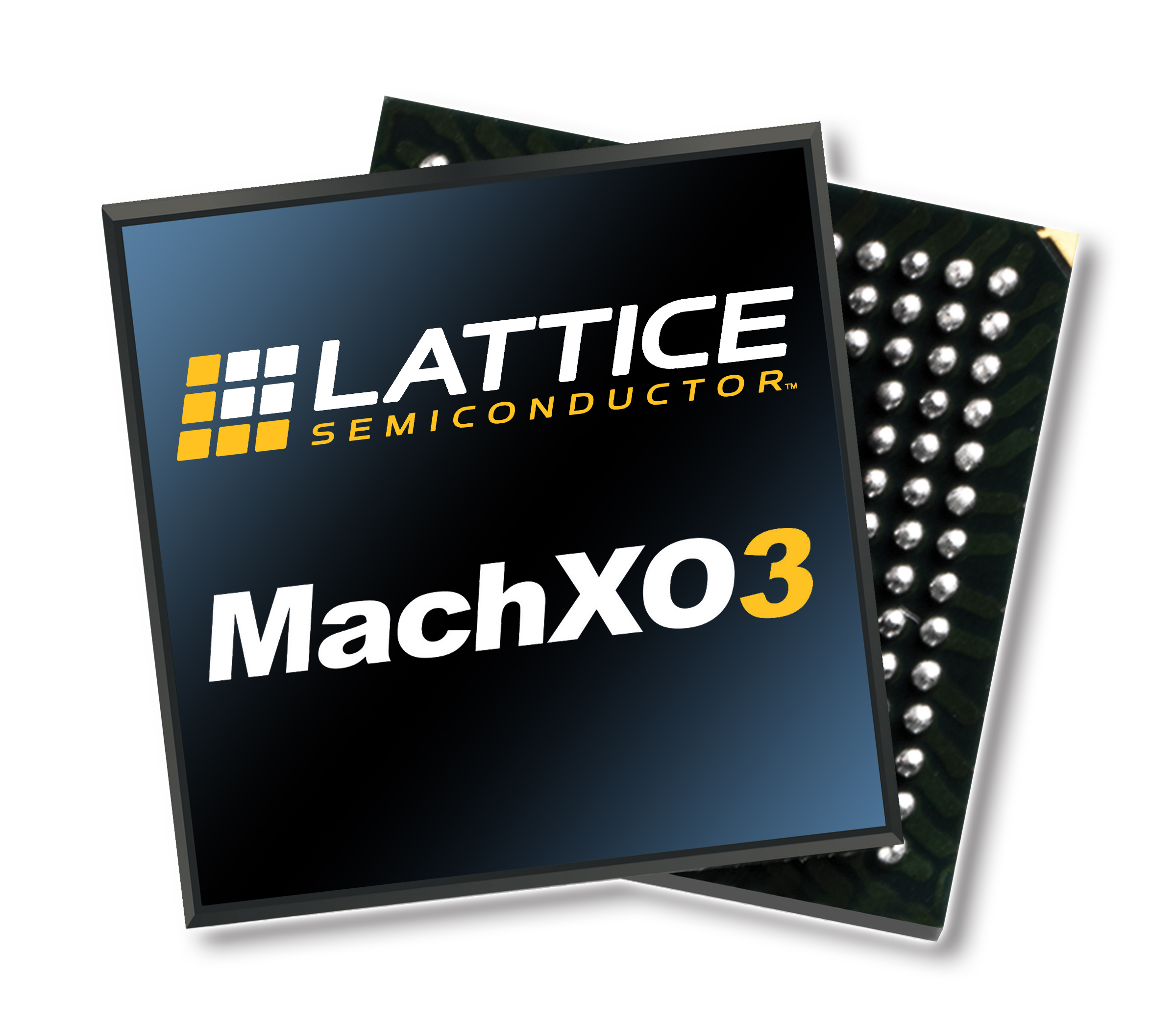
New Version of Lattice Diamond® Design Tool Enables Enhanced Bridging Applications
Click-to-Tweet
• MachXO3 FPGA family supports bridging of image sensors and displays using MIPI D-PHY, CSI-2 or DSI interfaces
• New Lattice Diamond 3.6 software update enables support up to 900 Mbps
PORTLAND, OR – October 26, 2015 – Lattice Semiconductor Corporation (NASDAQ: LSCC), the leading provider of customizable smart connectivity solutions, today announced that their award winning MachXO3™ family of devices supports 900 Mbps per lane operation for MIPI D-PHY interfaces, enabled by the latest Lattice Diamond 3.6 design tool suite software update. MachXO3 devices can now be used to bridge a wide variety of image sensors & displays with MIPI D-PHY, CSI-2 or DSI interfaces at speeds of up to 900 Mbps.
Lattice Diamond design software is a complete suite of FPGA design tools with an easy-to-use interface, efficient design flow, superior design exploration and more. The new software release, version 3.6, will enable MachXO3 customers to design more powerful yet still low power, small form factor FGPA bridging and I/O expansion solutions.
“Our MachXO3 FPGAs are becoming popular choices for image sensor and LCD bridging solutions in cameras, displays and machine vision applications,” said Shyam Chandra, senior product marketing manager at Lattice Semiconductor. “In addition, the production-proven MachXO3 family delivers the industry’s lowest power, smallest package sizes, and lowest cost per I/O, making these devices best suited in server, communication, and industrial applications.”
MachXO3L and MachXO3LF devices can now be used for bridging HD (1920×1080@60fps) and WQHD (2560×1440@60fps) displays as well as 4K@60fps with a wide variety of image sensors and processors. The MachXO3 family is available in Wafer Level Chip-scale packages (0.4mm ball pitch) and Flip-chip-BGA (csfBGA package 0.5mm Ball pitch) that are ideal for high performance, small form-factor applications.
More information about the MachXO3 family of FPGAs and Lattice Diamond FPGA design tool suite are available at www.latticesemi.com.
About Lattice Semiconductor
Lattice Semiconductor (NASDAQ: LSCC) is the global leader in smart connectivity solutions, providing market leading intellectual property and low-power, small form-factor devices that enable more than 8,000 global customers to quickly deliver innovative and differentiated cost and power efficient products. The Company’s broad end-market exposure extends from consumer electronics to industrial equipment, communications infrastructure and licensing.
Lattice was founded in 1983 and is headquartered in Portland, Oregon. In March 2015, the Company acquired Silicon Image, which is a leader in setting industry standards including the highly successful HDMI®, DVI™, MHL® and WirelessHD® standards.
For more information, visit www.latticesemi.com. You can also follow us via LinkedIn, Twitter, Facebook, or RSS.
Lattice Semiconductor Corporation, Lattice Semiconductor (& design), L (& design), Lattice Diamond, MachXO3, MachXO3L, and specific product designations are either registered trademarks or trademarks of Lattice Semiconductor Corporation or its subsidiaries in the United States and/or other countries.
MIPI is a registered trademark owned by the MIPI Alliance.
GENERAL NOTICE: Other product names used in this publication are for identification purposes only and may be trademarks of their respective holders.
For Further Information:
Sherrie Gutierrez
Lattice Semiconductor
408-616-4017
sherrie.gutierrez@latticesemi.com


