Phill Christie from imec IC-link talked to three experts from imec IC-link’s IP & Design Partnership Program: Ramses Valvekens from system-on-chip design company Easics, Jeroen Van Ham from analog and mixed-signal design company ICsense, and Bart Keppens from Sofics, a provider of intellectual property (IP) for electrostatic discharge protection. Together, they take a snapshot of what is needed to innovate with hardware in today’s substream markets.
Until recently, building hardware was not cool. With lengthy development cycles and a huge upfront investment for custom ICs, innovators have long turned to software to develop new products. But today a new generation of hardware hipsters has arrived. They build today’s smart systems that interact intelligently with their environment. Systems for small innovative markets, which they can deliver faster, more flexible, and with lower upfront investments.
Is hardware cool again?
For at least the last two decades, custom integrated circuits were implemented in leading edge technologies with development cycles longer than the shelf-lives of the products. It was punishingly expensive if you made a design mistake, and the upfront investments needed for leading edge silicon technology were eye-watering. Developing these custom ICs was therefore almost exclusively the playing field of large multinational semiconductor companies with deep pockets. Innovation in the global markets of consumer, computing, telecom and mobile was necessarily characterized by generation after generation of incrementally better products, based on IP-portfolios that took large teams several years to develop.
But today’s new generation of hardware hipsters are pushing the boundaries of what you can do with hardware; with systems that perceive their surroundings and start thinking about their environment with their cloud-based brains. Commenting on this, Joi Ito, director of the MIT Media Lab, said that “hardware is the new software” and that hardware start-ups are looking a lot like the software start-ups of the previous digital age. They are aggressively targeting innovative new Internet Of Things (IoT) markets, such as life sciences and medical diagnosis, automotive, security, vision and imaging, and industrial applications. These are rapidly growing, much more segmented and with a need for specialized lower-volume ASICs. So here the economies of scale which favor larger companies do not play.
Progress, change and innovation under these conditions does not follow schedules or five-year plans. It occurs through the rapid, dynamic, collective interaction across borders and time zones. The rise of these hardware hipsters, interacting with other startups in the new growth markets is referred to as substream innovation. It is new, definitely cool, and it is changing the way innovation is done in this era of the Internet of Everything.
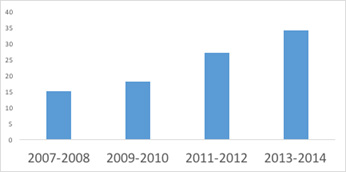
Fig 2: Number of IC-link projects in the areas of security, medical & wearables, radio access, and imaging & vision systems. Between the years 2011 and 2014, the number of projects in these areas approximately doubled.
The anatomy of silicon IoT applications
Admittedly, investment and media interest are drawn to the possibilities of huge data collections generated by the new wireless, perceptive systems. But to turn physical data into bits, you need hardware, and you need it to be smart and accurate. Here are a few aspects where the new hardware hipsters make a difference.
“A typical IoT product consists of several digital and analog components that need to be interconnected, packaged and protected from the harsh environments encountered in day to day life,” says Jeroen Van Ham from ICsense. “Unlike the digital world, in the analog world there is no real advantage in using the latest deep submicron technology nodes. In fact, there is little silicon area to gain because analog circuits usually don’t scale with shrinking transistor sizes. For an analog designer, in most cases it is even harder to design the same low-noise circuit in a smaller node because of the lower power supply voltage, which leads to less dynamic range. As a result, in a typical interface application, the preferred node still is 0.18um (either plain CMOS or a specialty flavor for high-voltage support). There is no use in trying to map a complex analog sensor interface to a state-of-the-art foundry process node; it is a waste of money.”
As for the digital side, the incremental NRE (non-recurring engineering) cost for integrating digital components is often small compared to an analog-only chip. The resulting unit production cost of an integrated digital solution can therefore be significantly lower than that of (multi-chip) alternatives. “However,” adds Ramses Valvekens, “Few successful chips never get updated. In the new, fast-moving markets, it is key to make digital designs future-proof. With scalable, dynamic designs, it becomes possible to roll-out a real product road map for a chip. At Easics, we succeed in doing that by parametrizing designs and by generating and assembling them using custom-designed hardware generators and Hardware Description Languages (HDLs). Such designs can be efficiently targeted towards different technologies, scaled and reused, in whole or in parts, in follow-on versions and derived products.”
In many new designs, the traditional analog IP buy-in model doesn’t fit well. Take MEMS (micro electro-mechanical systems) sensors, often an essential component in smart hardware. These sensors are becoming smaller and cheaper, thereby producing more (Brownian) noise and making them less sensitive to physical inputs. But end-customers keep demanding the same resolution and accuracy. As a result, the challenge is passed on to the circuit level. Initially to the circuit’s analog-front-end, and subsequently to digital signal processors. Available analog IPs are generic, maybe programmable to some extent, but not co-designed with the sensor and the reference circuits that are required at system level. As a result, the traditional analog IP buy-in model where a set of IPs is glued together in a chip will result in a sub-optimal system. Instead of working with standard component analog IP, a much better approach is to work with proven topologies (whose functionality is already proven in silicon) and fine-tune them for the application’s sweet spot.
A last and equally essential aspect that the new hardware hipsters have covered is electrostatic discharge (ESD), electrical overstress (EOS) and latch-up. Bart Keppens from Sofics says that what he has learned by supporting innovative startups is that many of the applications require non-standard on-chip ESD/EOS protection clamps, which are not always covered in mass-produced designs. “For example, the driving voltage of the implanted chip to restore hearing for (near) deaf people is in the order of 20V, much beyond the typical I/O interfaces provided by the foundry or I/O providers. Similarly, small signals (order of a few mV or mA) captured by sensors for motion detection and touch remain hidden in the noise or are lost due to leakage. Moreover, the probability of ESD stress is much higher as they are operated in harsh environments. For example, the plastic of your smartphone cover rubbing on the cloth of your back-pocket can generate very high voltages just millimeters away from very sensitive components, such as high-speed USB ports.”
Enabling low-cost prototyping and small-volume production
For substream innovators, unlike for larger companies, achieving the lowest possible unit production cost is not the first concern. They can reduce the production unit cost later on, once the product is on the market and customers turn out to buy more products than anticipated. Their game plan centers on producing truly innovative and high-margin products for niche markets, with the potential to grow into larger, more mature markets.
Instead, when a startup or an innovative SME implements an IoT product involving a custom chip design, the go/no-go decision is typically taken by private or venture capital investors and dominated by the required amount of upfront investment (NRE cost), the time-to-market, and the ability to precisely define the chip’s requirements.
“That is where IC-link and its design partners may help,” says Ramses Valvekens. “They can help lower the NRE costs and shorten the time to market through their extensive IP and know-how. In addition, together with the customer, they will help define and focus the chip requirements.”
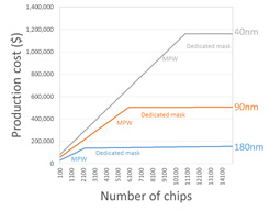
One essential factor included in the NRE is the initial cost of the lithographic mask set needed to process the wafers. These can cost, even for mature technologies, in the range of 100,000s of dollars. Especially to lower these high NRE cost for SMEs, foundries have introduced multi-project wafers (MPWs) and made these accessible through partners such as imec IC-link. In MPWs, designs of many customers share space on the same mask, but with hard limits imposed on the maximum number of chips per wafer, and the total number of wafers that can be ordered. For very small production runs measured in the thousands, mature MPW technologies offer extremely low initial costs, as low as 10,000s of dollars for a batch of approximately 100 prototypes of 32 mm2. Below figure illustrates the impact that MPW processing has on small volume production, as well as the change in the cost model when higher production volumes require a transition to a dedicated mask.
The new hardware hipsters – Fig 3
Substream innovation is here to stay
The convergence of high-growth, fragmented, wirelessly connected application domains characterized by manufacturing sweet spots using mature technologies has led to an explosion of activity by SMEs. New product ideas can be generated by small teams of people and taken quickly to small volume production and are no longer only the domain of large international corporations. Imec IC-link and its partners have committed to support this process, by providing infrastructure, design and IP assistance.
Hardware is cool again and we encourage everyone to discover their inner hardware hipster.